When you use your smartphone or laptop, it is easy to forget the sheer absurdity of the physical reality underneath. Behind that seamless experience lies centuries of effort from physicists, chemists, mathematicians, engineers, programmers, and designers. Inside your device is a slice of literal rock, purified to near perfection and carved with microscopic circuits. By just controlling the flow of electrons inside these circuits, we are able to make the rock calculate, remember, and think for us, sparing us the mental effort. A single operation takes less than a nanosecond, allowing your device to perform billions of calculations in the time it takes you to blink. This all works so seamlessly that, as users, we are spared from all the complexity, freeing us to simply focus on the task at hand.你手握智能手机,或启笔记本电脑,浑然不觉其下藏着多少天工开物之巧。那顺滑如水的体验背后,是物理学家、化学家、数学家、工程师、程序员与设计师数百年心血所聚。你指尖所触,不过一片经千锤百炼、几近纯澈的岩石,上面刻有微不可察的电路。只需操控这些电路中电子的流向,我们便能让这块顽石代我们计算、记忆、乃至思索,省去自身诸般脑力。一次运算尚不及一纳秒,在你眨眼之间,它已完成数十亿次演算。这一切运转得如此浑然天成,以至于作为使用者,你我皆不必过问其中繁复,得以心无旁骛,只专注于眼前之事。

Yet, while we can ignore how it all works underneath, doing so is becoming increasingly difficult as software dominates more of our lives. In fact, the digital world now influences our daily decisions just as much as the physical world. Just as we learn the basics of physics or biology to understand the physical environment, understanding software has become essential to navigate our digital environment. Without this basic literacy, we risk being passively managed or exploited by systems designed to capture our time and attention, preying on the anxieties that stem from not knowing how they work. With this understanding and clarity, we gain the agency to use technology better, make informed decisions about our digital safety, and even build software for our own specific needs.然而,我们可以置底层原理于不顾,软件却日渐浸透生活,要完全无视已是越来越难。如今数字世界对我们日常决断之影响,实不亚于物理世界。正如我们修习物理、生物以明周遭环境,通晓软件亦成为驾驭数字疆土之必需。若无此基本素养,便难免沦为后台系统所操纵与利用的对象——那些专为攫取你我时间与注意力而设的机制,正利用“不知其所以然”的焦虑乘虚而入。唯有洞察其理、了然于胸,方能收放自如,善用技术,在数字安危前做出明断,乃至依自身所需,亲手构筑软件。
My aim with this article is to strip away the “magic” in software and computers, showing that understanding how they work is not a privilege locked behind a computer science degree. To do this, I will avoid jargon as much as possible, introducing only the necessary concepts and building them up using first-principles thinking. Under the hood, computing is not a dry list of technical specifications, but a fascinating story of human ingenuity and practical problem-solving, where each new layer builds upon the last. By following this story, you can build clear mental models, gaining better clarity on what happens behind the scenes when you use your device. You’ll understand not just how the technology functions, but also the invisible safeguards built in to protect you. I have kept this article as concise as possible, retaining only the necessary historical context needed to show how these ideas took shape.我写此文,意在剥去软件与计算机身上的那层“魔法”外衣,让人人皆知:理解其理并非计算机科学学位持有者的特权。为此,我尽量避免术语堆砌,只引入必要概念,并以第一性原理层层推演。究其根本,计算并非枯燥的技术规格清单,而是一段人类巧思与实践解难交相辉映的佳话,每一层新筑皆立于前一层基石之上。循着这条脉络,你能在心中构建清晰的认知图景,明了每次操弄设备时幕后究竟发生了何事。你不仅知其功用,亦能窥见那些默默护你周全的隐形屏障。行文力求简明,仅保留必要的历史脉络,以彰显这些思想的来龙去脉。
Manipulating Physics to Do Our Math驾驭物理,为我演算
Most of our problem-solving in the world involves mathematical calculations, whether it is predicting the weather, calculating flight paths for planes, or checking the structural integrity of bridges. Originally, “computers” were just rooms full of mathematicians performing these calculations by hand, and some calculations took days. During wartime and the space race, the stakes grew even higher, calculating the trajectories of ballistic missiles and space rockets required solving thousands of complex equations. Since even a minute error could cause a rocket to explode, send a missile off target, or lead to the collapse of a bridge, these calculations had to be verified again and again. This process was very slow, expensive, and error-prone.世人遇事求解,多半离不了数理演算,无论预测天时、推算航迹,还是勘验桥梁之结构稳固。起初,“计算机”仅指满屋埋头苦算的数学家,有些演算一耗便是数日。及至战时与太空竞逐,情势更是十万火急:弹道导弹与运载火箭之轨迹,需解算万千繁复方程。然差之毫厘,谬以千里,一丝误差便足以令火箭凌空炸裂、导弹偏离靶标,或致桥梁倾覆。故同一组算式需反复核验,此道既缓且费,又极易出错。

There was an urgent need for a machine that could perform calculations reliably and quickly. Scientists searched for physical processes that could simulate counting, and one such early attempt was the mechanical calculator, built from interlocking gears and levers. But it had problems of its own, mechanical parts wear out over time, require constant maintenance, and are fundamentally slow.彼时亟需一台能快速而可靠地演算的机器。科学家们遍寻能模拟计数之物理过程,其中之一便是以齿轮与杠杆交相啮合的机械计算器。然此法亦有自身弊病:机械部件日久磨损,须时时养护,且从根本上就快不起来。

The simulator below demonstrates the fundamental building block of the mechanical calculators: a row of numbered wheels, one per decimal place (Hundreds, Tens, and Ones), exactly like the odometer in a car. Adding one turns the Ones wheel forward by one digit. When it rolls over from 9 to 0, a carry pin engages and pushes the Tens wheel forward by one digit. If the Tens wheel was itself at 9, its own carry pin engages too, dragging the Hundreds wheel along in the same motion, every wheel meshed through a carry pin turns together.下方模拟器所演示的,正是机械计算器最基本的构件:一排数字轮,各对应一个十进位(百位、十位、个位),与汽车里程表如出一辙。每加一,个位轮便向前拨动一格;当它由9翻转为0时,一枚进位销便切入啮合,推动十位轮前进一格。若十位轮恰也在9,其进位销同样触发,顺势将百位轮一并拨转——各轮借进位销相扣,同进共退。
Note that the wheels aren’t in constant contact like ordinary gears (that would lock them all to the same rotation speed); the carry pin only reaches in and engages the next wheel for that brief instant once every ten turns. We could support larger numbers by adding more wheels, and you can imagine how we could do other computations by changing the direction of rotation or adding more mechanical parts.须知这些轮子并非如寻常齿轮般时刻啮合(否则转速将被牢牢锁死);进位销仅在每转十格那一瞬,探入衔接次轮。若要应付更大数目,只需添轮即可;至于其他运算,亦可借反转轮轴或增设机件来实现,想来不难领会。
The real leap came when we moved from mechanical parts to electricity, employing electrical switches as our basic building blocks. We aren’t talking about the physical light switches in our homes, but rather switches controlled automatically by applying voltage. An electrical switch has two states: open (no current flows, representing 0 or false) and closed (current flows, representing 1 or true).真正的飞跃,在于弃机械而取电,以电气开关为根本之材。此开关非家中墙上那种手动的电灯开关,而是靠施加电压自动操控的。其态有二:断开时电流不通,代表0或假;闭合时电流奔涌,代表1或真。
By wiring these switches together in different ways, we can make logical decisions. The most fundamental of these configurations are called logic gates:将这些开关以不同方式接线,便可做出逻辑决断。其中最基础的几种配置,便称作逻辑门:
- AND gate (Series): If we place two switches one after the other, electricity only flows if Switch A AND Switch B are closed.与门(AND gate,串联):若将两开关首尾相接,则唯有开关A与开关B同时闭合,电流方能通过。
- OR gate (Parallel): If we place two switches side by side, electricity flows if Switch A OR Switch B is closed.或门(OR gate,并联):若将两开关并排放置,则开关A或开关B任一闭合,电流即通。
- NOT gate: A switch designed to be “normally closed” (letting current through by default), which disconnects and cuts off the current only when voltage is applied to it.非门(NOT gate):常态下闭合(默认导通),仅在施加电压时才断开,切断电流。
We can use a combination of these three gates to build any logical rule, no matter how complex. Think of any logical rule as a table mapping combinations of inputs to an output (either ON or OFF). To recreate this table using hardware, we only need to focus on the rows where the output is ON.凭这三种门的组合,便能构建任意复杂的逻辑规则。任取一条逻辑规则,皆可视作一张输入组合与输出(开或关)对照之表。要以硬件复刻此表,只需盯住输出为“开”的那几行即可。
To build a circuit for any ON row, we use an AND gate to detect that exact combination of inputs. If an input is supposed to be OFF in that row, we run it through a NOT gate first. This flips the OFF signal to ON, satisfying the AND gate (which only fires when all of its inputs are ON).要为某一“开”之行构建电路,须用与门来侦测该行的准确输入组合。若某输入在此行中应为“关”,则先令其过一道非门,将“关”翻转为“开”,如此方足与门之渴——毕竟与门只在所有输入皆为“开”时才会触发。
Finally, since the overall output should turn ON if the first target combination OR the second combination is met, we feed all the row detecting AND outputs into a single OR gate.末了,既然只要满足第一组目标组合“或”第二组组合,整体输出便应为“开”,故将所有侦测各行的与门输出,一并汇入一个或门之中。
Because every logical rule can be represented as a table, and any table can be built using this exact method, the trio of AND, OR, and NOT is mathematically complete, capable of representing any logical rule imaginable.盖因任一条逻辑规则皆可化作一张真值表,而任何真值表皆可以上述法门铸就;是以与、或、非三门联手,数学上便已完备无缺,足以表达一切可想象的逻辑规则。
To see this in action, the simulator below builds the XOR (Exclusive OR) rule, which turns the output ON only when the inputs are different. As we will see in the next section, this is the exact logic needed to perform binary addition.欲观其效,请看下方模拟器所搭建的异或门(XOR,Exclusive OR):唯有输入相异时,输出方为“开”。而在下一节中我们便会看到,二进制加法所倚仗的,正是这一逻辑。
Since switches only have two states, we cannot represent numbers using our usual ten digits (0 to 9). Instead, we use binary (base-2), which relies entirely on 0 and 1 (each digit is called a bit, short for binary digit).开关既只有两种状态,我们便无法以惯常的十个数字(0至9)来表示数目,转而采用二进制(base-2),全凭0与1行事(每一位称作bit,即binary digit,二进制位)。
Counting in binary works exactly like the mechanical gear counter, but with only two digits. In our familiar decimal (base-10) system, adding forces a rollover to with a carry of , forming . In binary (base-2), because is the highest digit, adding forces an immediate rollover to and carries . It is written as (which represents the decimal number ).二进制计数与机械齿轮计数器之理相通,只是数码仅余两个。我等熟悉的十进制(base-10)中,9加1便翻转为0,并向高位进1,写作10₁₀。至于二进制(base-2),因1已是最大数码,故1加1亦即刻翻转为0、进位为1,写作10₂(即十进制之2₁₀)。
To see how these switches perform math, let’s look at what happens when we add two single-bit numbers, and :欲见这些开关如何演算,且看两个单位数A与B相加:
- (Sum: , Carry: )0₂ + 0₂ = 00₂(和:0₂,进位:0₂)
- (Sum: , Carry: )1₂ + 0₂ = 01₂(和:1₂,进位:0₂)
- (Sum: , Carry: )0₂ + 1₂ = 01₂(和:1₂,进位:0₂)
- (Sum: , Carry: )1₂ + 1₂ = 10₂(和:0₂,进位:1₂)
Notice the patterns:细观其中规律:
- The Sum digit is
1only when one input is on but not both. This is exactly the behavior of an XOR (Exclusive OR) gate.和位仅在两输入恰有一个为1时置1,此正是异或(XOR)门之行为。 - The Carry digit is
1only when both inputs are on. This is exactly the behavior of an AND gate.进位位仅在两输入同时为1时置1,此正合与门(AND)之行为。
The simulator below wires the XOR circuit you just built, together with an AND gate, into this half-adder: toggle A and B to see the sum and carry bits update together.下方模拟器将刚才搭建的异或电路与一道与门组合,拼成一副半加器(half-adder)。你不妨拨动A、B开关,看和位与进位如何同步变化。
By wiring these gates together and feeding the carry output into the next bit’s input, we can add binary numbers of any size. This is called a ripple-carry adder, the carry from bit 0 cascades into bit 1, which may itself produce a carry into bit 2, and so on down the chain before the final sum is stable. Since subtraction is just adding a negative number, and multiplication is repeated addition, every arithmetic operation reduces to combinations of these basic gate circuits.将这些门电路级级相连,把进位输出发送至下一位的输入端,便能对任意长度的二进制数求和。此即所谓的行波进位加法器(ripple-carry adder):第0位产生的进位涌入第1位,第1位若再生进位,又泻入第2位,如此层层传递,直至结果归于稳定。既然减法不过加上一个负数,乘法亦只是重复相加,故一切算术运算,归根结底皆可化归为这些基础门电路的组合。
In early computers, we implemented these switches using vacuum tubes. They resembled sealed glass lightbulbs, containing a heated filament and a metal plate sealed inside a vacuum. Heating the filament gives its electrons enough energy to boil off into the vacuum, a process called thermionic emission, and the positively charged plate pulls them across the gap. A third element, a wire mesh grid, sits between the two. Applying a negative voltage to it repels the electrons back before they can cross, cutting off the current; releasing that voltage lets them flow again. This is a fast switch with no moving parts.早期计算机中,人们以真空管(vacuum tube)来实现这些开关。其形如密封的玻璃灯泡,内部置有发热灯丝与一块金属板,共处真空之中。灯丝受热,电子便获足够能量而逸出真空,此即热电子发射(thermionic emission);带正电的金属板则吸引电子跨越间隙。其间另设第三极——一圈金属栅网。若对其施加负电压,电子未及跨越便被斥回,电流立断;若撤去负压,电子复又畅流无阻。如此一来,开关之快,竟无需任何机械部件。

But as engineers tried to build larger, more capable machines, they hit a physical bottleneck. Vacuum tubes were bulky, consumed immense energy, and failed constantly. To innovate further, they couldn’t just optimize the fragile glassware; they had to go back to physical fundamentals and invent a better switch. This led to the invention of the first transistor in 1947, a solid-state electronic switch that was smaller, cooler, and far more reliable than vacuum tubes. That first device proved a solid piece of material could switch current with no vacuum and no hot filament.然工程师欲造更大、更强之机器时,却撞上了物理之壁。真空管体大笨重,耗电量惊人,且动辄损坏。要进一步突破,光在脆弱的玻璃器皿上修修补补已是无济于事,唯有回归物理根本,另觅更佳开关。于是,1947年首款晶体管(transistor)应运而生。此乃固态电子开关,较真空管更小巧、更清凉、亦更可靠。它首次证明,一块实心材料竟也能导断电流,既不需真空,亦无需炙热灯丝。
The refined design used in virtually every chip today came later, voltage is applied to a gate electrode sitting on a thin insulating layer above the silicon. That voltage generates an electric field that reaches through the insulator and pulls the silicon’s own electrons up to its surface, forming a thin conductive channel between two terminals, the source and drain; removing the voltage collapses the channel and cuts the current, switching current on or off with no moving parts at all.今日通用之改良设计更为精妙:于硅晶上方覆一层薄绝缘介质,其上置一栅极电极。施加电压时,电场穿透绝缘层,将硅体内电子吸至表面,遂于源极与漏极之间形成一道纤薄的导电沟道;撤去电压,沟道消散,电流立断——仅凭电场调度,片甲不动,便可开关自如。

Over the following decades, as we developed methods to print thousands of these transistors directly onto a silicon wafer, we created the integrated circuit (or chip). The size and spacing of these printed transistors is referred to as the process node (or manufacturing process), measured in nanometers (nm). The smaller the process node, the smaller each transistor, allowing us to squeeze more of them into the same physical space. Today, the smartphones in our hands pack a tremendous amount of computing power and memory while consuming only a fraction of the energy of early supercomputers, which occupied entire rooms and generated massive amounts of heat.此后数十年间,人们发明出将成千上万个晶体管直接印制于硅晶圆上的方法,由此诞生了集成电路(integrated circuit,即芯片)。这些晶体管的尺寸与间距称为制程节点(process node),以纳米(nm)计。节点愈小,晶体管愈微,同样空间便可容纳更多。如今你我掌中之智能手机,已蕴藏堪比往昔超级计算机的庞大算力与存储,而能耗仅及其零头;须知那些早期的庞然大物动辄占据整间屋子,散热更是汹涌如潮。
Translating Reality to Bits译现实为比特
We have seen how two-state switches allow us to represent and calculate numbers using the binary system. But we don’t want to restrict ourselves to just numbers and logic; most of our reality doesn’t arrange neatly as numbers. For example, sound is a continuous fluctuation of air pressure. Early telephone lines carried sound by translating the physical vibrations of a speaker’s voice into equivalent fluctuations in electrical voltage (using a microphone diaphragm), and doing the reverse at the listener’s end (using an electromagnet and speaker). But how do we represent this continuous, fluctuating electrical wave using logic gates?前文已述,藉由双态开关与二进制,我们得以表示并演算数字。然人之所欲不止于数字与逻辑;世间万物,多半并不会自行排成整齐的数字。譬如声音,本是空气压力的连绵起伏。早年电话线传递声音,靠的是将说话者声带的物理振动转化为相应的电压波动(借麦克风振膜),在收听端再逆向还原(借电磁铁与扬声器)。但这条连续起伏的电波,要如何才能用逻辑门来表达?
The insight came when scientists at Bell Labs, pioneers of communication technology, hit a bottleneck with telephone lines. They couldn’t send multiple signals simultaneously as they would interfere with each other. They also had to use amplifiers at different points to compensate for the signal weakening over distance. Noise could be introduced by any environmental interference, and amplifiers would boost even the noise. They realized that sending voice as a continuous analog wave was not that reliable, and there had to be a better way.这一洞见源自贝尔实验室的科学家——彼时通信技术之前驱。他们在电话线路上遇到瓶颈:多路信号同时发送便会彼此搅扰;沿途又需以放大器补偿信号随距离衰减;而环境干扰随时引入噪声,放大器却将噪声一并放大。他们逐渐意识到,以连续的模拟波传送语音并不那么可靠,必另有更佳蹊径。
Claude Shannon, a mathematician at Bell Labs, formalized this transition in his 1948 foundational paper on Information Theory. He popularized the term “bit” (binary digit) and, building on earlier work by Harry Nyquist, established the sampling theorem: if you sample a continuous analog signal at a high enough frequency, taking discrete measurements at regular intervals, you can digitize it and reconstruct it perfectly at the destination. The number of bits used per sample, the bit depth, determines how many discrete quantization levels are available: 1 bit gives 2 levels, 8 bits gives 256. At relay points along the line, an analog amplifier boosts both the weakened signal and any accumulated noise together. A digital regenerator does something better, it reads each incoming pulse, decides which level it represents, and retransmits a clean copy, discarding all noise in the process.贝尔实验室数学家克劳德·香农于一九四八年发表信息论奠基之作,将“bit”(二进制位,binary digit)一词广行于世,并承继哈里·奈奎斯特先前之研究,确立了采样定理:若以足够高的频率对连续模拟信号采样,亦即在固定间隔截取离散测量值,便可将其数字化,并于接收端完美重建。每一样本所用位数,即量化位深(bit depth),决定了离散量化层级之多寡:1位得2级,8位得256级。若以模拟放大器沿途中继,衰减的信号与累积的噪声会被一同放大;而数字再生器(digital regenerator)却更妙:它读取每一道传入脉冲,判定其所代表层级,再转发一份洁净之副本,整个过程将噪声尽数摒除。
Play with the simulator below, tweaking noise and other parameters to see how sampling and quantization reconstruct analog waves and filter out transmission noise.请试着操作下方模拟器,调节噪声与其他参数,观察采样与量化如何将模拟波重建,并滤除传输中的噪声。
Measuring Digital Information度量数字信息
Once we represent information as binary bits, we need units to measure it. A single bit (0 or 1) is too small to be useful on its own, so we group them, and each unit is easiest to remember by what it typically holds:信息既已化作二进制位,便需单位以度量之。区区一位(0或1)太过渺小,不堪大用,故将其分组;每个单位最好记的方法,便是看它通常能装下什么:
- Byte: a group of 8 bits, giving possible values — enough to store a single text character (like the letter
A).字节(Byte):8位一组,可得2^8 = 256种取值,足以存下一个文本字符(如字母A)。 - Kilobyte (KB): about a thousand bytes (or in binary convention) — a page of plain text.千字节(Kilobyte, KB):约一千字节(按二进制惯例实为1,024字节)——大抵一页纯文本。
- Megabyte (MB): about a million bytes — an MP3 song or a high-resolution photo is a few megabytes.兆字节(Megabyte, MB):约一百万字节——一首MP3乐曲或一张高分辨率照片,通常占数MB。
- Gigabyte (GB): about a billion bytes — a high-definition movie or a video game.吉字节(Gigabyte, GB):约十亿字节——一部高清电影或一款电子游戏。
- Terabyte (TB): about a trillion bytes — a modern hard drive stores one or two.太字节(Terabyte, TB):约一万亿字节——如今一块硬盘大概能存上一两个TB。
Now that we can represent reality as bits and bytes, how do we build a machine to process them?现实既可绎为比特与字节,试问如何构建一台机器来处理它们?
Building the Universal Computer构建通用计算机
In the earliest computers, the hardware was the program. To perform a specific task, such as calculating the trajectory of an artillery shell, engineers had to configure a custom physical circuit. Changing the task meant physically rewiring the connections or flipping heavy switches, a tedious process that required immense time and effort and was highly prone to error.最早的计算机中,硬件本身就是程序。若要执行特定任务——比如推算炮弹弹道——工程师必须搭建专属的物理电路。一旦任务变更,便得重新接线,或扳动笨重的开关,过程冗长繁复、耗时费力,且极易出错。
The breakthrough was the stored-program computer. Before it, machines like the ENIAC (Electronic Numerical Integrator and Computer, 1945) had to be physically rewired between tasks, operators plugged and unplugged cables to reconfigure the circuits for each new problem.突破之机在于“存储程序计算机”(stored-program computer)。在此之前,像ENIAC(电子数值积分计算机,1945年)这样的机器,每换一种任务便要重新布线;操作员须亲手插拔缆线,以重新配置电路。

In 1837, Charles Babbage had designed a mechanical general-purpose computer, the Analytical Engine. Its architecture consisted of a mill (a mechanical computation unit that performed addition, subtraction, and so on), a store (stacks of interlocking vertical gear wheels representing digits), and programs on punched cards. But it was never completed. Ada Lovelace, collaborating with Babbage, wrote what is considered the first algorithm intended for the machine and recognized that it could manipulate symbols, not just numbers.1837年,查尔斯·巴贝奇设计了一台机械式通用计算机——分析机(Analytical Engine)。其架构包含一座“磨坊”(mill,负责加减等机械运算的演算单元)、一处“仓库”(store,由相互啮合的竖直齿轮堆叠而成,以表征数位),以及以打孔卡片承载的程序。惜其终未完成。与她合作的阿达·洛芙莱斯写下了公认的第一套意在运行于该机器之上的算法,并洞察到:这台机器所操纵的不止于数字,亦可及于符号本身。
A century later, Alan Turing proved theoretically that a single Universal Turing Machine could simulate any computation by reading instructions from memory. John von Neumann’s 1945 architecture turned this into a concrete design, a CPU (Central Processing Unit, also referred to as a processor) that reads both data and instructions from the same memory over a shared bus. A bus is just a set of wires allowing data transfer between the components of a computer or any external devices. Virtually every computer built since follows this structure.一个世纪后,艾伦·图灵从理论上证明,只需一台通用图灵机(Universal Turing Machine),便能凭从存储器中读取指令来模拟任何计算。1945年,约翰·冯·诺依曼将这一构想化为具体架构:CPU(中央处理器,亦称处理器)经由一条共享总线(bus),从同一片存储器中既读取数据,又读取指令。所谓总线,不过是一组导线,负责在计算机各部件或外设之间输送数据。时至今日,天下计算机几无不循此结构。
Instead of hardwiring a specific circuit for a single type of calculation, we build a general-purpose processor with standard logic circuits that can be reused for different operations. We tell the processor what to do by feeding it operation codes (or opcodes).与其为某一类演算烧录死电路,不如打造一台通用处理器,内置标准的逻辑电路,以备不同操作反复调用。我们只需向处理器输送操作码(opcode),便可发号施令。
How does a binary number like 0001 physically activate a circuit? It does so through an instruction decoder, a circuit made of logic gates. For example, a decoder for a 2-bit opcode has gates wired to detect specific combinations, one gate fires only when it sees 00, another only for 01, and so on. When a specific gate fires, it acts as a physical router that sends electrical current to the corresponding part of the CPU, like opening the path to load data from memory or activating the addition circuit.诸如0001这样的二进制数,如何在物理层面激活电路?靠的是指令译码器(instruction decoder),一种由逻辑门搭成的电路。譬如一个2位操作码的译码器,其内部各门接线各不相同,专司侦测特定组合:一道门仅在遇到00时触发,另一道仅在01时触发,依此类推。当某道门被激活,它便充当物理路由器,将电流引向CPU中相应的部件——或开启通路以从存储器载入数据,或启动加法电路。
All the circuits described so far are combinational, their output is a pure function of their current inputs, with no memory of the past. The moment an input changes, the output changes. This raises an obvious question, how does a circuit hold a value over time, remembering its state even after the input signals are removed? Without this ability, a processor cannot execute multi-step instructions, run loops, or store intermediate results.前文所述诸般电路,皆为组合逻辑(combinational):输出纯由当前输入决定,不记前尘;输入一变,输出即变。这便引出一个大问题:电路如何才能将某一数值恒常保持,即便输入信号撤去,仍能记住自身状态?若无此能,处理器便无法执行多步指令、运行循环,更遑论储存中间结果。
The solution is feedback. Take two NOR gates (NOT-OR, which output a 1 only when both inputs are 0) and wire each gate’s output into the other gate’s input. The result is an SR latch, named for its two inputs, Set (forces the stored value to 1) and Reset (forces it to 0). Try the two buttons below, turning Set on drives the output to 1, and because that output loops back as an input to the other gate, the 1 keeps re-confirming itself even after you turn Set back off. That self-sustaining loop is the memory. The latch exposes this stored bit as , alongside its opposite, (read “Q-bar”), which is handy elsewhere in the circuit whenever the negated value is needed.解题之钥在于反馈。取两枚或非门(NOR gate,NOT-OR:仅当两输入皆为0时方输出1),将各门的输出回接至另一门的输入。如此便得SR锁存器(SR latch),其两输入分别名为Set(置位,强制存储值为1)与Reset(复位,强制为0)。请试按下方按钮:按下Set,输出Q即变为1;此输出又绕回成为另一门之输入,自行不断确认,纵使你松开Set,1亦自维持。这自循环便是记忆。锁存器将存储的位以Q端示人,同时给出其反相Q̅(读作“Q-bar”),电路别处若需反值,正好取用。
Now try turning both Set and Reset on at once. Both gates get forced to 0, so and stop being opposites, breaking the one guarantee the latch is supposed to provide. Worse, whichever one you turn off last decides the final state, an outcome that depends on tiny, unpredictable timing differences rather than your input. This is the SR latch’s fundamental flaw, Set and Reset must never both be 1.此刻你不妨将Set与Reset同时按下。两门皆被强置为0,Q与Q̅便不再互为反相,锁存器赖以立足的唯一保证就此崩解。更要紧的是,最终状态取决于你松开哪一个稍晚半瞬——而这半瞬之差既微小又不可预期,非输入本身所能掌控。这便是SR锁存器的根本缺陷:Set与Reset断然不可同时为1。
To close off that flaw, we build a D flip-flop (where D stands for Data) on top of the same latch. Instead of exposing Set and Reset directly, we derive them from a single input , so Set only ever equals and Reset only ever equals its opposite, . Since and can never both be 1, Set and Reset can never both be 1 either, the forbidden state is designed out entirely.为堵此漏洞,人们在同一锁存器之上再加一层,造就D触发器(D flip-flop,D即Data)。它不再直接暴露Set与Reset,而是从一个单一输入D推演而出:Set始终等于D,Reset始终等于D的反相D̅。既然D与D̅绝无可能同时为1,Set与Reset亦永无同真之日,禁地遂被从根本上根除。
To coordinate when this update happens, we gate it behind a clock signal, a control wire that steadily pulses between 0 and 1 like a heartbeat. The flip-flop only updates on the precise rising edge of a clock tick (the transition from 0 to 1, represented as ) rather than continuously. This is why an SR latch is called level-triggered (its output tracks its inputs the whole time they’re active) while a D flip-flop is edge-triggered (it grabs ‘s value only at that instant and holds it, ignoring any changes to until the next tick).若要统摄更新之时机,则引入时钟信号(clock)作门控:它如心跳般节律分明,在0与1之间往复脉动。触发器仅在时钟上升沿(由0跃至1之瞬,以↑记之)精准采数,而非随时变动。是以SR锁存器称作电平触发(level-triggered):输入有效期间,输出始终追随输入;而D触发器则称边沿触发(edge-triggered):仅在那一瞬攫取D值并锁住,此后D无论如何变化,亦要待下一拍方再理会。
This is the fundamental single bit storage element. A register is simply a bank of flip-flops, one per bit, used by the CPU to hold the numbers it is actively calculating.此乃单比特存储之根本元件。寄存器(register)不过是由一排触发器并立而成,每位一器,供CPU暂存当前正在演算之数。
By scaling this storage concept up, wiring millions of these basic memory cells into a massive, addressable grid; we get main memory (commonly known as RAM, or Random Access Memory).将此存储之念层层放大,将数百万枚这样的基本记忆单元缀成一张庞大而可寻址的网格,我们便得到了主存储器(main memory),通常称为RAM(随机存取存储器)。
Notice, though, that this memory has a fundamental limitation, the latch’s feedback loop only holds its bit while current flows through the gates. Cut the power, and every bit in RAM vanishes. Memory built this way is called volatile.然此记忆有一根本限制:锁存器的反馈环路唯有在电流贯通时方能持位。一旦断电,RAM中每一位便如梦幻泡影,即刻消散。如此筑就的存储器,称为易失性存储(volatile)。
For data that must survive a power off, your photos, documents, and the programs themselves; we need storage (also called secondary storage), devices that record bits in a physical state that persists without power. Hard drives do this by magnetizing microscopic regions on a spinning platter; modern SSDs (Solid State Drives) do it by trapping electrons inside insulated flash cells. Storage is vastly larger and cheaper per byte than RAM, but also thousands of times slower to access.若要数据经得起断电——你的照片、文档,乃至程序本身——则需外存(亦称辅助存储,secondary storage)。此类设备将位记录于无需通电即可长存的物理状态中:硬盘借磁化旋转盘片上的微观区域以存之;现代SSD(固态硬盘)则将电子囚于绝缘闪存单元之中。外存容量浩瀚,每字节之价远低于RAM,然读取之慢,亦相去千百倍。
This speed gap creates a division of labor that explains much of what you experience daily, programs and files live in storage, and are copied into RAM to be worked on. Launching an app means loading its instructions from the drive into memory; saving a document means writing it back from memory to the drive. It’s why unsaved work is lost when a program crashes, while saved files survive even a total power failure.这般速度之别,催生了日常分工:程序与文件栖于外存,用时再抄入RAM以供操弄。启动应用,不过是从硬盘将指令载入内存;保存文档,则是将内存中的数据写回硬盘。是以程序崩溃时,未存之稿便付东流;而既已存盘之文件,纵遇整机断电,亦安然无恙。
This raises a chicken and egg question, if RAM is empty at power on and programs must be loaded into RAM to run, what loads the very first program? The answer is a small third kind of memory, a ROM (Read-Only Memory) chip whose bits are permanently fixed during manufacturing. The CPU is hardwired to start executing from the ROM’s address the instant power arrives. The small program stored there, called firmware, does just enough work to find the drive and copy the operating system (the core software that coordinates the computer) from storage into RAM, then hands over control. Every boot up you have ever watched is this chain running: ROM, then firmware, then the operating system loading into memory.这里便有个“先有蛋还是先有鸡”的难题:若开机时RAM空空如也,而程序又须载入RAM方能运行,那么谁来加载这第一个程序?答曰:一种小巧的第三类存储器——ROM(只读存储器)芯片,其位值在出厂时便已永久固化。CPU被硬接线为通电瞬间即从ROM的固定地址起开始执行。其中所存的那段小程序名曰固件(firmware),只消完成一件事:寻得硬盘,将操作系统(即协调整机运转的核心软件)从外存抄入RAM,然后交权。你每一次按下开机键所见的启动过程,便是这一链条依次运转:先ROM,继以固件,再载入操作系统。
With a way to store not just temporary calculation results, but also long lists of instructions, we finally have everything needed to implement the stored-program computer. We no longer need to physically rewire the machine to change its task. Instead, we can change the computer’s behavior simply by loading a new sequence of instructions into memory. This is the leap that created software. (While a specific sequence of instructions designed for a task is called a program, software is the broader term representing these programs and the data that controls the hardware.)既能暂存演算结果,又能长列指令存于一处,我们终于凑齐了实现存储程序计算机所需的一切。再也不必手执焊线去改机器使命,只消将新指令序列载入内存,计算机的行止便随之而变。正是这一跃,催生了软件。(若说程序program是针对某一任务的特定指令序列,则软件software乃更宏阔之称,统摄这些程序以及一切驾御硬件的数据。)
Every processor consists of three core components:每一枚处理器皆由三大核心部件组成:
- The control unit: reads instructions from memory and directs the flow of electricity to activate specific circuits.控制单元(control unit):从存储器中读取指令,并调度电流走向,以激活特定电路。
- The ALU (Arithmetic Logic Unit): a bundle of logic gates that performs calculations.算术逻辑单元(ALU, Arithmetic Logic Unit):一束逻辑门之集,专司运算。
- The registers: immediate, high-speed storage slots.寄存器(registers):供即时周转的高速存储槽。

These components interact with external memory over a set of shared wires called the bus. The processor executes a continuous loop: fetch an instruction from memory over the bus, decode it, and execute it in the ALU, writing the results to registers. This loop runs billions of times per second.这些部件经由一组共享导线——即总线(bus)——与外部存储器交互。处理器周而复始地执行同一循环:经总线自存储器取指、译码、交由ALU执行,再将结果写入寄存器。此循环每秒运转数十亿次。
A tiny crystal oscillator, a slice of quartz that vibrates at a highly precise frequency when electricity is applied (just like in your wristwatch), emits an electrical pulse at a fixed frequency we call the clock speed, measured in gigahertz (GHz). Each pulse marks the boundary of one cycle, and each cycle advances the fetch-decode-execute loop by one step. A 3 GHz CPU completes roughly three billion of these steps per second.机内有一小块晶体振荡器,乃一片石英薄片,通电后以极高精度震颤(正如腕表中之石英)。它以固定频率发放电脉冲,此频率即为时钟速率(clock speed),以吉赫兹(GHz)计。每一脉冲标志着一个周期之界限,推动取指-译码-执行之轮前进一步。一枚3 GHz的CPU,每秒大约完成三十亿步这样的操作。
In reality, modern processors are vastly more complex than this simple sequential model. To bypass physical speed limits, they use pipelining (overlapping the fetch, decode, and execute stages of multiple instructions like an assembly line), out-of-order execution (running instructions as soon as their input data is ready, regardless of their order in the code), and branch prediction (guessing which way a conditional jump will go to keep the pipeline full). They also rely on layers of high-speed cache memory because fetching from external RAM takes hundreds of cycles. However, this sequential model remains the fundamental logical abstraction that programmers write for.然而实际上,现代处理器远比这种简单的顺序模型复杂。为突破物理速度之限,它们引入了流水线(pipelining):如工厂流水线般将取指、译码、执行各阶段交叠并行;乱序执行(out-of-order execution):只要输入数据就绪,便即刻运行,不拘泥于代码中的原始次序;分支预测(branch prediction):猜测条件跳转之去向,务求流水线不空转。此外,它们还仰赖多层高速缓存(cache memory),因为从外部RAM取数动辄耗上数百个周期。不过,取指-译码-执行这一顺序模型,始终是程序员赖以思考的底层逻辑抽象。
To execute instructions sequentially, the CPU uses a special register called the program counter (PC). It holds the memory address of the next instruction to fetch. After each fetch, PC advances to the next address automatically. The fetched instruction is held in an instruction register (IR) while the control unit decodes it and routes electricity to the correct circuit.指令欲得循序而行,CPU 内有一特殊寄存器,名曰程序计数器(PC)。此寄存器中,静静存放下一条待取指令的内存地址。每取一指,PC 便自行递进,指向下一个地址。已取之指令,则暂存于指令寄存器(IR)之中,候控制单元拆解译码,引电流至相应电路,方得运转。
To repeat actions or make decisions, we use a jump instruction. Jumps overwrite PC with a target address. For conditional jumps, comparison instructions set a zero flag (Z) in the ALU. When two values are equal, Z becomes 1. A JNE (jump if not equal) instruction checks Z and only takes the jump if Z is 0. With just these mechanisms — sequential advance, comparison, and conditional jump — we can build any loop or branching logic. The simulator below shows a simple countdown timer, writing each value to a memory-mapped output address (where a write to a specific memory address physically triggers a peripheral 7-segment LED display).若需反复行事,或临机决断,则需借跳转指令之力。跳转者,乃以目标地址直接覆写 PC,令执行流改道而行。至若条件跳转,则有比较指令专司其事,于 ALU 中置一零标志位(Z)。两值若相等,Z 即置为 1。JNE(若不相等则跳转)之指令,便是查此 Z 位;唯有 Z 为 0 时,方跃然而起,跳转生效。仅凭此三者——顺序递进、比较判别、条件跳转——便可演化出万千循环与分支逻辑。下方模拟器中,便见一简易倒计时之例:每得一值,便写入内存映射之输出地址(往特定内存地址写入数据,于物理层面直接驱动外接之七段 LED 显示器)。
On our laptops and smartphones, we have a large grid of tiny, color changing light units called pixels (short for picture elements) instead of a simple 7-segment display. Just like the display in our simulator, a modern screen is controlled using memory-mapped addresses. The computer reserves a region of memory (called a framebuffer) where each address corresponds to a specific pixel coordinate on the screen. Drawing a user interface is simply the CPU writing color values to these addresses fast enough that they appear as a smooth, moving image.我等膝上电脑与掌中手机之屏,早已非简陋七段显示器可比,而是由无数微小发光单元——像素(pixel,即 picture element 之缩写)——铺成巨幅网格,逐一点染颜色。与模拟器中之显示相仿,现代屏幕亦借内存映射地址操控。计算机特辟一片内存区域,名曰帧缓冲(framebuffer),其中每一地址,皆对应屏幕上特定像素之坐标。绘制界面,无非便是 CPU 以极高速度向这些地址写入色彩数值,令一幅幅画面连绵映出,遂成流畅动态之影像。
Each pixel’s color is encoded as three separate bytes, red (R), green (G), and blue (B); each ranging from 0 to 255. By mixing these three intensities, the display hardware produces any color. So the framebuffer stores 3 consecutive bytes per pixel, R at one address, G at the next, B at the one after. Each tiny pixel contains three even tinier subpixels, one per channel, whose physical light-emitting elements blend together at normal viewing distance into the single color you see.每一像素之色,皆以三字节分置,红(R)、绿(G)、蓝(B),各以 0 至 255 为域。以此三色强度交相调和,显示硬件便可幻化出任意颜色。故帧缓冲中,每像素占连续三字节:R 居其首地址,G 随其后,B 又次之。每一微小像素之内,更藏三枚纤毫子像素,各应一色通道;其物理发光元件于寻常视距之外交融混色,遂成人眼所见之唯一色彩。
So far, information has only flowed outward, from memory to the screen. Input travels the same bus in reverse. When you press a key, the keyboard sends an electrical signal called an interrupt to the CPU. The CPU pauses its fetch-decode-execute loop, jumps to a small handler routine that reads the key’s code from the device (over memory-mapped addresses, just like the display, but reading instead of writing), stores it, and resumes exactly where it left off, all in less than a microsecond. A mouse click, a touch on the screen, or data arriving from the internet reaches your programs the same way. The interruption is invisible to the running program, yet it is how every input you make finds its way in.至此,信息之流皆由内向外,自内存奔往屏幕。然输入之道,却循同一条总线反向而行。当你按下键钮,键盘即发一电信号,名曰中断(interrupt),直抵 CPU。CPU 当即暂停其取指-译码-执行之循环,跳转至一小段处理例程,自设备读取按键之编码(经由内存映射地址,与显示器同出一辙,唯彼处为写入,此处为读取),将其存妥,随即回到原处,续接前缘;整个过程耗时不足一微秒。鼠标点击、屏幕触控,抑或网络数据送达,皆循此道进入程序。此中断之于运行中的程序,几不可察,然你之每一输入,皆赖此方得入门。
This completes the machine, a processor executing instructions, memory holding both program and data, and interrupt-driven pathways for output and input. Before we climb to the next layer, it is worth seeing where the hardware story itself went next. Engineers pushed clock speeds aggressively through the 1990s, but above roughly 4 GHz, the chip dissipates more heat than can be removed. Rather than fighting the heat, the industry moved to multiple cores, several independent processors on one die, each running its own instruction stream. More cores don’t make a single sequential task faster; they allow more tasks to proceed in parallel.如此,整机方成:处理器负责执行指令,内存兼储程序与数据,复有中断驱动之通路,以司输入输出。欲更上层楼之前,不妨先览硬件之后续演进。上世纪九十年代,工程师竭力推高时钟频率,然至约 4 GHz 之上,芯片散热之剧,已非现有手段可除。与其硬撼热力,业界遂转向多核:同一块晶圆之上,集成数枚独立处理器,各自行其指令流。核数增多,并不能令单一串行任务更快,却可令诸多任务并行推进。
When general-purpose scaling slowed, the industry pivoted again, this time toward specialized silicon. Instead of one processor design that handles everything, modern chips dedicate regions of the die to specific workloads, GPUs (Graphics Processing Units) run thousands of simple calculations in parallel, and neural accelerators are purpose-built for the matrix arithmetic behind AI models. These circuits trade the CPU’s flexibility for raw throughput on one class of problem, and that trade is what made training and running today’s AI models feasible. The pattern from the vacuum tube repeats, hit a physical wall, then change the approach rather than pushing harder against it.通用扩展既缓,业界再度转身,此番直指专用硅片。不再以一款处理器包打天下,现代芯片转而于晶圆之上划分疆界,各司其职:GPU(图形处理器)可并行执行数千简单运算;神经网络加速器专为 AI 模型背后之矩阵算术而生。这些电路舍却 CPU 之百般灵活,换取单一类问题上之纯粹吞吐;正因有此取舍,训练并运行今日之 AI 模型方才成为可能。真空气管时代之覆辙昭然:遇物理之壁,不若改弦更张,而非一味蛮进。
None of this means the transistor is near retirement. Quantum computers, despite the headlines, are not faster general-purpose computers; they are a fundamentally different kind of machine that exploits quantum effects to attack a narrow class of problems, such as simulating molecules or factoring the large numbers behind certain encryption schemes, and they would be useless for running your browser. For everything described in this article, the transistor remains the foundation, and engineers keep advancing it, stacking components vertically, refining transistor geometry, and packaging multiple specialized dies into a single chip.凡此种种,并非意味晶体管已近暮年。量子计算机纵占头条,却并非更快的通用计算机;其本为截然不同的机器,借量子效应专攻狭窄领域,诸如分子模拟或破译特定加密方案背后之大数分解,若用以运行浏览器则全无用处。本文所述之一切,晶体管仍是根基;工程师亦未曾止步,或垂直堆叠元件,或精研晶体管几何,或将多枚专用芯片封装于一体。


Writing Software in English用英语编写软件
A processor only understands binary. Writing software originally meant manual lookup of binary opcodes. To simplify this, programmers wrote a translation program called the assembler. It maps human-readable mnemonics (like ADD i) directly to their binary equivalent.处理器只识二进制。最初编写软件,意味着手工查寻二进制操作码。为化繁为简,程序员遂编写了一种翻译程序,名曰汇编器(assembler)。它将人类可读之助记符(如 ADD i)径直映射为其二进制等价物。
Grace Hopper built the first compiler in 1952, the A-0, proving that programs could translate human-readable code into machine instructions automatically, a concept widely doubted at the time.1952 年,Grace Hopper 造出首款编译器 A-0,证明了程序亦可自动将人类可读之代码转译为机器指令;此念在当时,实乃众所质疑之事。
This created a compounding feedback loop. Early compilers were hand-written in assembly, but once a language became expressive enough, its own compiler could be rewritten in that language, a process called bootstrapping, making the compiler self-hosting. The C compiler is written in C. The Go compiler is written in Go. Software was now being used to build better software.由此便生出一股滚雪球般的反馈循环。早期编译器以汇编手书而成,然一旦某门语言表意足够丰富,其编译器便可转而以该语言自身重写,此过程名曰自举(bootstrapping),令编译器成为自托管(self-hosting)。C 编译器以 C 写成,Go 编译器以 Go 写成。软件自此开始用于构建更优之软件。
The same principle extended to hardware. Designing a chip with billions of transistors by hand is not a realistic possibility. Engineers describe circuits using hardware description languages (like Verilog), simulate them in software, and use Electronic Design Automation (EDA) tools to automatically generate the physical layout. The Intel 4004 in 1971 had 2,300 transistors, possible to verify by hand. The Apple M1 has 16 billion. The chip design tools that made that possible are themselves software, running on earlier chips. Without software, we could not design the hardware that runs software.同一原理亦延伸至硬件。以手工设计一枚集成数十亿晶体管之芯片,实非人力可及。工程师以硬件描述语言(如 Verilog)描绘电路,以软件仿真验证,再借电子设计自动化(EDA)工具自动生成物理布局。1971 年之 Intel 4004 仅有 2,300 枚晶体管,尚可以人工核验;Apple M1 则达 160 亿枚。能成此功绩之芯片设计工具,本身亦是软件,运行于更早世代之芯片之上。无软件,则无法设计运行软件之硬件。
Because assembly is tied to the physical design of a specific chip, code written in one processor’s assembly will fail to run on another. To solve this, we created high-level languages like C, Fortran, or Python. These languages let us express logic using familiar abstractions, like variables, loops, and functions instead of registers and jumps.汇编既与特定芯片之物理设计紧密相连,则为一处理器所书之汇编代码,换至另一处理器便无法运转。为解决此弊,人们发明了 C、Fortran、Python 等高级语言。这些语言使人得以借熟悉之抽象表达逻辑,诸如变量、循环、函数,而无需再与寄存器、跳转纠缠。
At this level, programming is less about managing hardware and more about designing algorithms, step-by-step logical instructions to solve a specific problem (like sorting a list of names or finding the shortest route on a map). An algorithm is the abstract concept, while a program is the concrete implementation of that algorithm in a specific programming language (the logic implemented in C or Python). By writing code in a language closer to human speech, software becomes far easier to write, read, and maintain.到了这一层,编程之要义已非驾驭硬件,而是设计算法——解决特定问题之逐步逻辑指令(譬如为名单排序、或于地图寻最短路径)。算法乃抽象之概念,程序则是算法在特定编程语言中的具体实现(以 C 或 Python 落实之逻辑)。以更接近人言的代码书写,软件之编写、阅读与维护,自是事半功倍。
For example, the abstract algorithm for our countdown from the simulator is simple:譬如前述模拟器中之倒计时,其抽象算法甚是简明:
- Start with a number (5).自某数起算(5)。
- If the number is zero, stop.若该数为零,则止。
- Otherwise, subtract 1 and repeat from step 2.否则减 1,回到第 2 步重复。
To turn this algorithm into an executable program, we translate these steps into a programming language. In C, we can write it using a simple while loop:欲将此算法变为可执行之程序,便需将这些步骤转译为编程语言。以 C 言之,可借一简易 while 循环写就:
int x = 5;
while (x != 0) {
    x = x - 1;
}
The compiler translates this high-level loop into an equivalent sequence of assembly instructions like the ones we ran in the simulator, handling the registers and jumping details for us. To help you follow along, I have added explanatory comments next to the instructions (in assembly, any text after a semicolon is a comment, notes left by programmers to document the code for others, which the assembler ignores when processing the assembly code).编译器会将此等高级循环译为与模拟器中所运行相若之汇编指令序列,代你处置寄存器与跳转细节。为助你理解,我于指令旁添设注释说明(汇编之中,分号后之文字即为注释——程序员留予他人阅读之注解,汇编器处理代码时则会略去)。
; Assembly equivalent of the C loop above (with output)
LOAD  #5      ; Set initial value: acc = 5
loop:
STORE result  ; Save value to memory (output)
SUB   #1      ; Subtract 1: acc = acc - 1
CMP   #0      ; Compare accumulator to 0
JNE   loop    ; If not zero, jump to 'loop'
STORE result  ; Display the final 0
Play with the compiler mapping simulator below. Switch between the tabs to see how variables, math, loops, and conditionals in a high-level language are translated into low-level assembly instructions by the compiler.不妨亲自试玩下方之编译器映射模拟器。切换标签页,可见高级语言中的变量、运算、循环与条件语句,如何经编译器之手转译为底层汇编指令。
Consider reading a text file. In C, you must manually request a handle from the operating system to open the file, set aside a temporary block of memory (called a buffer) to hold the characters, read the bytes into it, and close the file when you’re finished.试以读取文本文件为例。在 C 中,你须亲自向操作系统申请句柄以打开文件,另辟一块临时内存(名曰缓冲 buffer)以容纳字符,将字节读入其中,事毕再关闭文件。
// Open the file "notes.txt" in read-only mode
FILE* file = fopen("notes.txt", "r");

// Set aside 256 bytes of memory to hold the text
char buffer[256];

// Read up to 256 bytes from the file into the buffer
fread(buffer, 1, 256, file);

// Close the file to free up system resources
fclose(file);To understand what is actually happening, every character stored in a file is mapped to a number using a standard encoding called ASCII (American Standard Code for Information Interchange). The letter H maps to 72, e to 101, and so on. A special byte, the newline (\n, value 10), marks where one line ends and the next begins. Say notes.txt contains the single line Hello. When C reads the file, it loads these raw bytes into the buffer in memory, one after another at sequential addresses.欲明其究竟,文件中存储之每一字符,皆依标准编码 ASCII(American Standard Code for Information Interchange)映射为数字。字母 H 对应 72,e 对应 101,余者类推。另有一特殊字节,即换行符(\n,值为 10),标示一行之终与下一行之始。假设 notes.txt 中仅含一行 "Hello"。当 C 读取此文件时,便将诸字节依次载入内存中之缓冲,一五一十,各居连续地址。
Writing these lines of code every single time we want to read a file would quickly become exhausting. To avoid repeating ourselves, high-level languages allow us to package instructions into reusable blocks called functions.每逢读文件便要重写这些代码,长此以往,不免令人疲惫不堪。为免重复劳作,高级语言允许我们将指令封装为可复用之块,名曰函数(function)。
A function is simply a named block of code that performs a specific task. By wrapping a sequence of instructions inside a function, we can run them all at once just by calling its name. For example, we can wrap our C file reading code into a custom function definition.函数者,无非一段具名之代码块,专职一事。将一连串指令包裹于函数之内,只需呼其名字,便可一次性尽数执行。譬如,可将前述 C 文件读取代码封装为一自定义函数。
char* read_file(char* filename) {
    FILE* file = fopen(filename, "r");
    // Allocate 256 bytes of memory dynamically to hold the text
    char* buffer = malloc(256);
    fread(buffer, 1, 256, file);
    fclose(file);
    return buffer;
}
Now, anyone wanting to read a file doesn’t need to know about file handles, buffers, or byte offsets. They can simply call the function and free the memory when finished:至此,凡欲读文件者,皆无需理会文件句柄、缓冲区或字节偏移。径直调用此函数即可,事后释放内存:
char* text = read_file("notes.txt");
// ... use the text ...
free(text); // Release the memory back to the system
That is what functions do, give a name to a procedure so you can reason at a higher level without holding the implementation details in your head.此即函数之功用:为一套工序命名,使你得以在更高层次上推理,无需将实现细节时时萦怀。
Python, as a higher-level language, takes this concept of abstraction way too seriously.Python 作为更高级的语言,于抽象之道可谓不遗余力。
text = open("notes.txt").read()One line compared to a complex, multi-step process in C. Python’s open().read() is still opening a file handle, growing a buffer as it reads until EOF, and releasing it afterward. The CPU is still doing the same work but the language handles the buffer management, resource cleanup, and all the error handling internally. While C is high-level compared to assembly, Python allows us to write programs at an even higher level of abstraction by managing memory and resource cleanup for us. This simplicity is why Python became so popular in academia and research. For instance, most machine learning code is written in Python, while the performance-critical parts underneath are written in C or C++ and called from Python.相较 C 中繁复多步之过程,Python 仅需一行。Python 的 open().read() 背后,仍是开启文件句柄、随读取增长缓冲、直至 EOF 再释放之一整套过程。CPU 所做之工并无二致,只是语言于内部代劳了缓冲管理、资源清理与全部错误处理。C 较之汇编已是高级,Python 则更进一步,代管内存与资源清理,使人得以在更高抽象层级上编程。正因这份简洁,Python 在学界与研究中风靡一时。举例来说,大多数机器学习代码以 Python 写成,而其下性能关键之部分则以 C 或 C++ 写成,再由 Python 调用。
To understand why there is such a performance difference between them, and why we still need C or C++ underneath Python for the heavy lifting, we have to look at a fundamental difference in how these languages execute. C is a compiled language. Before you run a C program, a compiler translates the entire source code into native binary machine code for your specific CPU. When you run it, the processor executes it directly at maximum speed.欲解二者性能差异之缘由,以及为何 Python 之下仍需 C 或 C++ 扛鼎负重,须观其执行方式之根本不同。C 乃编译型语言。运行 C 程序之前,编译器先将全部源码转译为你所使用 CPU 之原生二进制机器码。运行时,处理器直接执行,速度臻于极致。
Python, on the other hand, is an interpreted language. Instead of being translated ahead of time into native machine code, your script is handed to a program called an interpreter, which carries out each step itself. (The standard Python interpreter does first convert your script into a compact internal format called bytecode, but that bytecode is still executed by the interpreter, instruction by instruction, not by the CPU directly.) Think of it this way, with a compiled language like C, your code runs directly on the CPU. With an interpreted language like Python, your code is just input data for another program (the interpreter), and that extra layer of indirection on every single operation introduces performance overhead. That extra work is the price we pay for convenience.Python 则属解释型语言。它并非事先转译为原生机器码,而是将脚本交予一个名曰解释器(interpreter)的程序,由其逐步代行。(标准 Python 解释器虽会先将脚本转为一紧凑的内部格式,名曰字节码 bytecode,然此字节码仍由解释器逐条执行,而非由 CPU 直接处理。)不妨这般理解:编译型语言如 C,你的代码直接在 CPU 上奔腾;解释型语言如 Python,你的代码不过是另一程序(解释器)之输入数据,而每一次操作皆多此一层间接,自然引入性能开销。这份额外之工,便是为便利所付之代价。
C and Python are just two examples in a massive ecosystem of high-level languages. Today, we choose different languages depending on our needs: JavaScript or TypeScript for interactive web applications, Go for highly concurrent backend systems, and Rust for systems programming where performance and memory safety are both critical.C 与 Python,仅是庞大高级语言生态中之两例。今日,我们依需求择语言而用:JavaScript 或 TypeScript 用于交互式网页应用,Go 用于高并发后端系统,Rust 则用于那些性能与内存安全皆至关紧要之系统编程。
This choice is heavily guided by the cost of failure. In a typical web application, the stakes are relatively low; we can afford to make mistakes because a bug usually just means a broken page that can be fixed with a quick update. But if a bug occurs in an aircraft, a medical device, or a nuclear reactor, the consequences can be fatal. In safety-critical systems, we choose languages and engineering practices that prioritize strict compile-time verification, memory safety, and deterministic behavior, even if they are harder to write.此选择深受失败成本之左右。寻常网页应用之中,风险尚属有限;偶出纰漏,通常不过页面崩毁,推送修补即可。然若故障发生于飞行器、医疗仪器或核反应堆之中,后果便可能致命。于安全攸关之系统,我们选取语言与工程实践时,优先考量严格的编译期验证、内存安全与确定性行为,纵使其编写更为艰深。
Furthermore, programming in the modern world is rarely about writing everything from scratch. In almost any language, we can find pre-written code packages called libraries created by others. These libraries solve common problems for us, from parsing dates and making network requests to rendering complex 3D graphics, allowing us to build powerful software by assembling existing building blocks, freeing us to focus on our unique ideas.况且,当今之编程,鲜有从零写起者。几乎在任何语言中,皆可寻得他人预写之代码包,名曰库(library)。这些库代我们解决常见问题:解析日期、发起网络请求、渲染复杂三维图形,诸如此类。借组装既有积木以构建强大软件,我们得以腾出心神,专注于自身之独到构思。
Sharing the Processor and Memory Among Software在软件之间共享处理器与内存
Originally, computers ran only one program at a time, you waited for it to complete execution, and then loaded the next program. As hardware became more powerful, this was highly inefficient. The CPU would sit idle for seconds waiting for a human to type or for a slow disk to spin.初时,计算机一次仅能运行一个程序;须待其执行完毕,方载入下一个。硬件日强之后,此法低效之极:CPU 每每空等数秒,候人键入,或候慢速磁盘旋转。
To solve this, computer systems in the 1960s introduced time-sharing. At the time, computers were massive, room-sized central machines called mainframes shared by an entire organization. Instead of having their own processor, users worked at separate screens and keyboards called terminals wired directly to the mainframe, sharing its single CPU simultaneously. UNIX, developed at Bell Labs in 1969, built on this concept to create a unified operating system (OS) design, the background coordinator software that sits between applications and the hardware.为解决此弊,六十年代之计算机系统引入了分时(time-sharing)。彼时,计算机乃庞然巨物,一室之大,名曰大型主机(mainframe),供整间机构共用。用户并无各自之处理器,而是于称作终端(terminal)的独立屏幕与键盘前工作,直接连线主机,共享同一颗 CPU。1969 年贝尔实验室所创之 UNIX,即基于此理,构建出统一之操作系统(OS)设计——此乃坐镇于应用程序与硬件之间的后台协调软件。
However, early personal computers in the 1980s (running systems like MS-DOS) took a step backward. Because early desktop microprocessors were simple, they could still only run one program at a time. If an application crashed, it corrupted the memory of the entire system, forcing a hard reboot (and making turning it off and on again the standard troubleshooting protocol).然八十年代之早期个人电脑(运行如 MS-DOS 之系统)却不进反退。因早期桌面微处理器颇为简陋,一次仍只能运行一个程序。若某应用崩溃,便累及整片内存,逼使系统硬重启(这也令“关机再开机”成了标准排障之道)。
To bring UNIX-level stability and multitasking to the personal computer, we needed hardware-enforced boundaries. Modern CPUs solve this by supporting different privilege modes, controlled by a physical state in the processor itself. The core coordinator of the OS, the kernel, runs in a privileged kernel mode (giving it direct, unrestricted access to the physical hardware). Meanwhile, user programs run in a restricted user mode. In user mode, the CPU hardware physically blocks any direct access to hardware or memory; if a program needs to read a file or draw to the screen, it must execute a system call, a special instruction that triggers a hardware interrupt, handing control to the kernel to perform the task safely.欲将 UNIX 级别之稳定与多任务带至个人电脑,便需硬件强制之边界。现代 CPU 以支持不同特权级(privilege mode)来解决此题,此状态由处理器自身之物理机制所控。操作系统之核心协调者,即内核(kernel),运行于特权之内核模式(kernel mode),得以直接、无限制地访问物理硬件;而用户程序则运行于受限之用户模式(user mode)。于用户模式下,CPU 硬件直接阻断任何对硬件或内存的直接访问;若程序欲读取文件或绘制屏幕,必须执行系统调用(system call)——此一特殊指令触发硬件中断,将控制权交予内核,由其安全代劳。
To virtualize physical hardware for these user programs, the kernel relies on three primary abstractions:为给用户程序虚拟化硬件,内核仰赖三大抽象:
- Multitasking (CPU Virtualization): The OS shares a single CPU among multiple programs by rapidly switching between them. To prevent any single program from hogging the processor, a hardware timer regularly interrupts the CPU (the same interrupt mechanism that delivers your keystrokes), handing control back to the kernel. During this context switch, the kernel saves the current program’s registers, loads another program’s saved registers, and swaps execution. This happens so quickly that every program feels like it has sole possession of the CPU.多任务(CPU 虚拟化):操作系统借快速切换,令多程序共用一颗 CPU。为防止某一程序独占处理器,硬件定时器定期中断 CPU(与传递按键之中断机制相同),将控制权交还内核。于此次上下文切换(context switch)中,内核保存当前程序之寄存器,载入另一程序之已存寄存器,交换执行。此过程迅疾万分,令每一程序皆自以为独拥 CPU。
- Virtual Memory (RAM Isolation): To prevent programs from crashing into each other or reading sensitive data, the kernel isolates memory. Programs operate in a virtual address space. A hardware unit translates these virtual addresses to physical RAM on the fly. A program cannot access memory outside its allocated space.虚拟内存(RAM 隔离):为防止程序互相冲撞或读取敏感数据,内核将内存隔离。程序运行于虚拟地址空间(virtual address space)之中。一硬件单元实时将虚拟地址转译为物理 RAM。程序无法踏出其分配空间半步。
- The File System (Storage Abstraction): Instead of forcing programs to manage raw blocks or sectors on a physical drive, where file contents are actually stored as scattered blocks of bytes in permanent storage, the OS maintains a lookup table mapping file paths to their exact physical locations, presenting a clean hierarchical tree and handling access control behind the scenes.文件系统(存储抽象):操作系统不再强令程序直接管理物理驱动器上之原始块或扇区——文件内容实则以零散字节块存于永久存储之中——而是维护一张查找表,将文件路径映射至其确切物理位置,对外呈现为整洁之层级树,并于幕后操持访问控制。
By switching between privileged kernel mode and restricted user mode (often called running in user space), the OS ensures a single crashed application cannot take down the entire system.借内核模式与用户模式(常称运行于用户空间 user space)之切换,操作系统确保单一应用崩溃不致掀翻整台系统。
How we design around these crashes depends entirely on the system’s context. On a smartphone, an app crash is a minor inconvenience. But in safety-critical systems like spacecraft landers, flight control computers, or medical life-support devices, a software crash or memory corruption can be deadly. These environments require different safeguards: redundant hardware backups, formal mathematical verification of the code, and specialized real-time operating systems designed to guarantee that critical processes never fail or stall.如何应对此类崩溃,全然取决于系统之场景。智能手机上,应用崩溃不过略有不便;然于航天着陆器、飞行控制计算机或医疗生命维持设备等安全攸关之系统,软件崩溃或内存损坏皆可致命。此等环境需不同保障:冗余硬件备份、代码的形式化数学验证,以及专为确保关键进程永不失效或阻塞而设计的实时操作系统。
Making Computers Talk to Each Other让计算机彼此对话
The Internet began in 1969 as ARPANET (Advanced Research Projects Agency Network), a US defense research network designed to connect computers across the country. To do this, engineers had to solve a fundamental problem, how should data travel?互联网肇始于 1969 年之 ARPANET(Advanced Research Projects Agency Network),本为美国国防研究网络,旨在连接全国之计算机。为此,工程师须解决一根本难题:数据当如何传输?
Telephone networks of the time used circuit switching, which established a dedicated, continuous physical connection between two points for the duration of a call. But computers only send data intermittently, making a dedicated line highly inefficient. Instead, ARPANET pioneered packet switching. Under this design, data is split into small pieces called packets containing the payload and a destination address. Routers pass these packets hop-by-hop, each packet finding its own path. This made the network incredibly resilient, packets could route around failures, so no single broken link could sever the entire connection. TCP/IP (Transmission Control Protocol / Internet Protocol), adopted as the universal standard in 1983, became the common language that unified these individual networks into one global internet and the rest is history.当时之电话网络采用电路交换(circuit switching),于两点之间建立专属、持续之物理连接,通话期间独占线路。然计算机发送数据乃是断断续续,专属线路未免大材小用。ARPANET 遂开创分组交换(packet switching)。依此设计,数据被切为小块,名曰分组(packet),内含载荷与目的地址。路由器逐跳转发,各分组自行寻路。此举令网络极具韧性:分组可绕开故障路由,任一链路损毁亦不至切断全局连接。TCP/IP(Transmission Control Protocol / Internet Protocol)于 1983 年定为通用标准,成为统一诸网为一域互联网之共同语言,此后之事,便是尽人皆知之历史了。

To ensure reliable delivery over this best-effort system, we use a stack of protocols:为确保此尽力而为(best-effort)系统之可靠交付,我们仰赖一叠协议:
- IP (Internet Protocol) routes individual packets from machine to machine across the network, but makes no guarantee they arrive.IP(Internet Protocol)负责将单个分组于网络中自一机路由至另一机,却不保证必达。
- TCP (Transmission Control Protocol) sits on top of IP, numbering each packet and requiring acknowledgements so any lost packets are automatically resent, giving applications a reliable byte stream.TCP(Transmission Control Protocol)建于 IP 之上,为每组编号并要求确认;若有遗失,自动重发,向应用程序提供可靠字节流。
- HTTP (HyperText Transfer Protocol and its encrypted form, HTTPS) sits on top of TCP, defining a request-response format for fetching documents and data.HTTP(HyperText Transfer Protocol,及其加密形态 HTTPS)复建于 TCP 之上,定义请求-响应格式,以获取文档与数据。
The S in HTTPS stands for secure, and it is worth pausing on, because it is the most important everyday safeguard on the internet. Your packets pass through many machines you don’t control, the cafe’s Wi-Fi router, your internet provider, a dozen routers in between, and any of them could read or alter what passes through. So before sending data, your browser and the server perform an extra handshake to verify the server’s identity and agree on a temporary encryption key; from then on, all traffic between them is mathematically scrambled so that only the two endpoints can unscramble it. The machines in the middle can still see which server you are talking to, but not what you are saying: your passwords, messages, and card numbers travel through hostile territory unreadable. The padlock in your browser’s address bar simply means this machinery is active.HTTPS 中之 S,意为 secure(安全),值得驻足一观,因它乃是互联网上最紧要之日常防护。你的分组须穿越无数你无法掌控之机器——咖啡馆 Wi-Fi 路由器、网络服务商、途中数十台路由器——其中任何一环皆可读取或篡改流经之数据。故发送数据之前,浏览器与服务器先行一番额外握手,以核验服务器身份并商定临时加密密钥;自此而后,二者间全部流量皆经数学混淆,唯两端方可解之。中间机器仍能知晓你与何服务器对话,却无从窥见内容:密码、消息、卡号,皆于险地穿行而不露形迹。浏览器地址栏中之小锁,仅表示此机制正在运转。
The Web is a separate application built on top of this network, invented by Tim Berners-Lee in 1991. Where the internet moves packets between machines, the Web is a system of linked documents (pages) that any browser can retrieve and render. Each page is written in HTML (HyperText Markup Language), a set of tags that describes a document’s structure and content, which the browser parses to know what to draw. When you type an address, DNS (Domain Name System) translates the human-readable name to an IP address, your browser requests the files over HTTP/TCP, and the browser’s engine paints the pixels. Because web pages run code written by strangers, the browser enforces a sandbox, an isolated runtime that prevents page code from reading your local files or reaching your operating system directly.万维网(Web)则是构建于网络之上之独立应用,由 Tim Berners-Lee 于 1991 年发明。互联网只管在机器间搬运分组,万维网则是一套由链接串联之文档(网页)系统,任何浏览器皆可取来渲染。每页以 HTML(HyperText Markup Language)写成,以一组标签描述文档之结构与内容,浏览器解析后方知所绘。当你键入地址,DNS(Domain Name System)将此人类可读之名转译为 IP 地址,浏览器经由 HTTP/TCP 请求文件,再由浏览器引擎将像素逐一点亮。因网页运行陌生人所写之代码,浏览器特设沙盒(sandbox)——一隔离运行时,阻止页面代码读取本地文件或直接触及操作系统。
The browser also quietly became the most consequential software distribution platform in history. Before it, shipping software meant compiling separate installers for Windows and macOS, and convincing users to download and run executable files. When Google launched Chrome in 2008 with a new JavaScript engine called V8, fast enough to run real applications, it opened up a new wave of webapps. A developer could now write one codebase, deploy it to a server, and reach every device on the planet with a web address. Users get the latest version automatically on every visit with no installation step.浏览器亦悄然成为史上最具影响力的软件分发平台。在此之前,发布软件意味着须为 Windows 与 macOS 分别编译安装包,并说服用户下载运行可执行文件。2008 年 Google 推出 Chrome,携新 JavaScript 引擎 V8 而来,其速足以运行真正之应用,遂开启 webapp 新浪潮。开发者今可只写一套代码,部署于服务器,以一个网址触达全球每一台设备。用户每次访问,自动获取最新版本,无需安装。
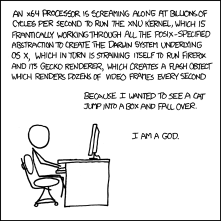
Web standards evolved to keep up. The early web was static text and images; rich multimedia required third-party plugins like Adobe Flash (early YouTube couldn’t stream video without it), until HTML5 brought native, hardware-accelerated video and audio playback into the browser itself.网络标准亦随之演进。早期之网止有静态文字与图像;欲得丰富多媒体,须借第三方插件如 Adobe Flash(早期 YouTube 若无它便无法串流视频),直至 HTML5 将原生硬件加速之视频与音频播放纳入浏览器自身。
Today’s browsers are massive, complex software platforms. They bridge the gap between web applications and the system by exposing APIs (Application Programming Interfaces), pre-defined sets of rules, functions, and protocols that allow different software programs to communicate with one another. Just as an operating system exposes APIs to let programs request services from the kernel, a modern browser exposes secure APIs that allow web applications to render real-time 3D graphics, read local files, or fetch data, all while keeping the application safely sandboxed.今日之浏览器,已是庞大而复杂之软件平台。它于网页应用与系统之间架桥铺路,对外暴露 API(Application Programming Interfaces,应用程序编程接口)——此乃预先定义之规则、函数与协议集,使不同软件得以互通。恰如操作系统暴露 API 以令程序向内核请求服务,现代浏览器亦暴露安全 API,令网页应用得以渲染实时三维图形、读取本地文件或获取数据,同时将其安全禁锢于沙盒之中。
Combined with the ability to run compiled languages at near-native speeds via WebAssembly, the browser has become the ultimate abstraction layer. It serves as the primary environment where we spend most of our computing time while the operating system runs silently in the background. Just like a secondary OS, the browser manages CPU scheduling and memory allocation for web apps running in separate tabs, isolating them from one another and restricting access to hardware resources without explicit permission. The web didn’t just connect computers; it evolved into a universal runtime that abstracted both the hardware and the OS underneath.复加之以 WebAssembly 之力,令编译型语言得以接近原生速度运行,浏览器遂成终极抽象层。它作为我等消耗大部分计算时间之主要环境,而操作系统则悄然退居幕后。宛如次级操作系统,浏览器为运行于各标签页中之 web app 调度 CPU、分配内存,彼此隔离,且未经显式许可不得触及硬件资源。万维网不仅连接了计算机,更进化为一种通用运行时,将底层硬件与操作系统一并抽象殆尽。
However, this convenience comes with a steep trade-off. By running inside a secure sandbox, web applications give up direct, low-level access to the underlying hardware and operating system APIs. Additionally, running software inside a browser means executing layers of virtual machines and rendering engines, introducing massive performance and memory overhead compared to native binaries. A browser tab running a simple web-based text editor might consume hundreds of megabytes of RAM to do what a native utility could accomplish in a few kilobytes. We traded raw execution efficiency and low-level control for near-zero distribution friction.然此便利亦伴随沉重代价。运行于安全沙盒之内,网页应用便放弃了对底层硬件与操作系统 API 的直接、低阶访问。此外,于浏览器内运行软件,意味着须执行层层虚拟机与渲染引擎,相较原生二进制文件,引入巨大之性能与内存开销。一个浏览器标签页运行简易之网页文本编辑器,或许消耗数百兆内存,而原生工具仅需数千字节即可成事。我们以原始执行效率与低阶控制,换取了近乎零摩擦之分发便利。
To see this entire multi-layered stack in action, consider what happens when a browser actually loads a page or a web app fetches data. While we write high-level code to trigger these actions, the underlying system must coordinate a complex routine of network protocols. For instance, before any HTTP data can be exchanged, TCP must establish a reliable connection. It does this through a three-way handshake: the browser sends a synchronization request (a SYN packet), the server replies with a synchronization-acknowledgment (SYN-ACK packet), and the browser sends a final acknowledgment back. Only after this handshake is complete can the actual data transfer begin.欲见此整套多层栈如何运转,不妨思索浏览器加载页面、或 web app 获取数据时究竟发生何事。我等虽以高级代码触发此等动作,底层系统却须协调一繁复之网络协议流程。譬如,在交换任何 HTTP 数据之前,TCP 须先建立可靠连接。它以三次握手达成:浏览器先发送同步请求(SYN 分组),服务器以同步确认应答(SYN-ACK 分组),浏览器再回以最终确认。唯有此握手告成,实际数据传输方可开始。
This entire sequence, DNS lookup, TCP handshake, HTTP request, and encrypted response is what a single line like requests.get("https://api.example.com/data") triggers in Python. The library handles all the finer details; the programmer sees one call and a result.这整串流程——DNS 查询、TCP 握手、HTTP 请求、加密响应——便是 Python 中一行诸如 requests.get("https://api.example.com/data") 所触发之内幕。库文件代为处置全部细枝末节;程序员眼中所见,唯此一调用与一结果。

When your browser makes a request, it reaches a server, a computer running continuously, waiting to respond to incoming connections. On this computer, web server software (like Nginx or Apache) listens for incoming HTTP traffic, handles encryption, and directs the request to our application code. This server machine is not fundamentally different from your laptop; it runs the same operating system abstractions we covered, just optimized for handling thousands of simultaneous connections rather than a single interactive user.当你通过浏览器发起请求时,信息便会抵达一台服务器——这是一台常年持续运转的计算机,只待响应接入的连接。这台机器上运行着Web服务器软件(如Nginx或Apache),会监听传入的HTTP流量、处理加密事宜,再将请求转交至应用代码。这台服务器与你日常用的笔记本电脑并无本质区别,运行的都是我们此前讲过的同一套操作系统抽象层,只是优化方向不同:它要应对的是数千条并发连接,而非单个交互式用户。
In practice, modern software rarely runs on one dedicated machine. It runs on cloud infrastructure, warehouse-scale data centers owned by a few large providers, where organizations rent virtual machines (VMs) rather than buying physical hardware. The same virtualization principle from the OS section applies here, a layer called the hypervisor lets many virtual machines share one physical server, each convinced it owns dedicated hardware. This gives smaller teams the ability to scale to millions of users without purchasing a single piece of hardware.实际应用中,现代软件极少只跑在一台专属机器上。它们运行在云基础设施之上——那是几家大型服务商拥有的、规模堪比仓库的数据中心,各组织租用其中的虚拟机(VM),而非采购实体硬件。我们在操作系统章节讲过的虚拟化原理在此同样适用:有一层名为hypervisor的组件,能让多台虚拟机共享同一台物理服务器,且每台虚拟机都确信自己独占着一套专属硬件。这般设计让小团队无需采购任何实体硬件,便能支撑起数百万用户的使用规模。
Most server-side software needs to persist and query structured data. This is handled by a database, software built specifically for storing records reliably and retrieving them efficiently. Databases are organized and queried using SQL (Structured Query Language), a language designed specifically to express operations like “find all orders placed by this user in the last 30 days.” Behind every form submission, social media post, or bank transaction is a database write. The disk, the file system, and the kernel are all still underneath; the database is simply a well-engineered abstraction over them.绝大多数服务端软件都需要持久化存储结构化数据、对其进行查询,这一功能由数据库承担。数据库是专门为可靠存储记录、高效检索数据而开发的软件。我们使用SQL(结构化查询语言)来组织、查询数据库,这门语言专为表达“查找该用户近30天下过的所有订单”这类操作而生。每一份表单提交、每一条社交媒体动态、每一笔银行交易背后,都是一次数据库写入操作。磁盘、文件系统、内核这些底层组件依然存在,数据库不过是构建在它们之上的一层精妙抽象罢了。
Today, there are many database engines to choose from. While relational databases like PostgreSQL or MySQL organize data in tables using SQL, non-relational (NoSQL) databases like MongoDB store data as flexible documents. Each is optimized for different workloads. To prevent data loss and handle massive scale, databases can also be configured with replicas, real-time clones of the database running on separate servers that can take over if the main database fails.如今市面上的数据库引擎种类繁多。PostgreSQL、MySQL这类关系型数据库用SQL将数据整理为表格形式存储,而MongoDB这类非关系型(NoSQL)数据库则将数据存为灵活的文档结构,二者分别针对不同的负载场景做了优化。为防止数据丢失、支撑海量规模,数据库还可配置副本——即运行在独立服务器上的实时克隆实例,一旦主数据库出现故障,副本便可立即接管。

You Can Only Control What You Understand唯所明者,方能掌控
Every layer in this stack is designed to be ignored when things are working as expected. This is the whole point of abstraction, it lets you reason about a problem without holding every layer beneath it in your head, freeing up mental bandwidth for the task at hand. Knowing which layer to think at for a given problem is crucial. You don’t descend unless the problem points you there, and the problem usually tells you where to look. But when it does require going deeper, you need an idea of what is below the abstractions you are currently working with, or it’s a shot in the dark. When debugging poor performance with no obvious issue in our high-level code, we might need to inspect lower-level interactions like system calls, tune database query plans, or identify memory leaks caused by unfreed allocations. Sometimes solving a problem means going all the way down to the foundations, like inventing the transistor when vacuum tubes could no longer scale.这套技术栈的每一层,本就是为了“运转如常时便可忽略”而设计的。这便是抽象的核心要义:它容你不必将底层的每一层细节都尽数记在脑中,便能理清问题逻辑,把心智余力留给当下要务。遇到问题时,清楚该在哪一层着手思考,是重中之重。除非问题指明要往下追查,否则不必贸然深入;而多数时候,问题本身自会告诉你该往何处寻。可若当真需要下探底层,你就得对你当前所用的抽象层之下的原理有个大致认知,否则便是瞎摸黑撞,全无头绪。比如调试性能问题时,若高层代码里找不到明显症结,我们就可能需要查看系统调用这类底层交互、优化数据库查询计划,或是揪出由未释放的内存分配导致的内存泄漏。
Other times it means branching off to a new path altogether. Go did this for highly concurrent programming. Operating systems let a single program run many tasks at once by splitting it into threads, independent instruction streams that the kernel schedules using the same context-switching we saw earlier, but each thread costs system calls and significant memory. Rather than building on OS threads directly, Go introduced lightweight goroutines that its own runtime multiplexes onto a small number of physical OS threads.还有些时候,这意味着要另辟蹊径。Go语言在高并发编程上走的便是这么一条新路。操作系统原本是通过将程序拆分为线程,实现单程序多任务并行运行——线程是独立的指令流,由内核用我们此前讲过的上下文切换机制来调度,但每条线程都会消耗系统调用开销与大量内存。Go没有直接基于操作系统线程搭建,而是推出了轻量级的goroutine,由其自身运行时环境将大量goroutine复用到少量物理操作系统线程之上。
Without an understanding of the underlying system, a software engineer has no real control over making software work the way they expect, whether that means optimizing its performance, guaranteeing its stability, or keeping it secure. They are entirely at the mercy of their chosen abstractions. Every layer in this article was built by someone who had a good understanding of the foundations. The transistor came from physicists who understood quantum mechanics. The compiler came from programmers who understood assembly and wanted a more portable, readable way to express programs. The operating system came from programmers who understood physical processors and memory, and wanted to share those resources securely and efficiently. Each new abstraction was built by people who could see through the one they were working on.若对底层系统没有了解,软件工程师便无法真正让软件按自己的预期运行——无论是优化性能、保障稳定性,还是确保安全性,都无从谈起。他们完全受限于自己选用的抽象层,毫无主动权。本文讲的每一层技术,都是由深谙底层原理的人打造出来的:晶体管来自懂量子力学的物理学家;编译器来自懂汇编语言、想找一种更易移植、更易读的方式来编写程序的程序员;操作系统来自懂物理处理器与内存、想安全高效共享这些资源的程序员。每一层新的抽象,都出自能看透其所构建的抽象层之下本质的人之手。
This continuous layering of abstractions illustrates a software-focused version of Jevons’ paradox. As technological progress makes computing resources (like CPU cycles and memory) more efficient and cheaper, we do not consume less of them. Instead, we use the savings to build more ambitious systems. History shows that new innovations rarely reduce our workload; they simply expand our horizons. Early programmers spent hours squeezing maximum performance out of slower processors and kilobytes of memory, and their hard constraints pushed the entire industry to design faster hardware and smarter operating systems. Today, our personal devices are packed with gigabytes of RAM, capacities those early pioneers could not have dreamed of; yet a single Chrome window can easily hog all of it. Rather than enjoying “infinite” resources, we consume massive amounts of memory and compute to run heavier frameworks, render rich user interfaces, and serve millions of concurrent users.这一层接一层的抽象堆叠,正是杰文斯悖论在软件领域的写照。随着技术进步,计算资源(如CPU周期、内存)愈发高效、愈发廉价,我们却不会因此减少消耗。相反,我们会把省下来的资源用来搭建更宏大的系统。历史早已证明,新技术极少能减轻工作负担,只会不断拓宽我们的想象边界。早年的程序员曾花数小时从慢速处理器和几KB的内存里榨取极限性能,他们面临的严苛约束,推动了整个行业去设计更快的硬件、更智能的操作系统。如今我们的个人设备都装上了数GB的内存,这是早年先驱们做梦都想不到的容量;可即便如此,一个Chrome浏览器窗口就能轻松占满全部内存。我们并未因此享受“无限”资源,反而消耗海量内存与算力,去运行更重的框架、渲染更丰富的用户界面、服务数百万并发用户。
The same paradox is now repeating one level up, with the production of software itself. As AI agents make generating code dramatically cheaper, we won’t write less software; we will write far more of it, more prototypes, more personal tools built for an audience of one, more ambitious systems that were previously too expensive to attempt. And all of that new software still runs on the same stack described in this article, and still needs to be understood, debugged, and secured by someone.同一悖论如今正往上一层重演,体现在软件生产本身。随着AI智能体让代码生成的成本大幅降低,我们不会写更少的软件,反而会写出更多:更多原型、更多为单人受众打造的私人工具、更多此前因成本过高而不敢尝试的宏大系统。而所有这些新软件,依然运行在本文所讲的同一套技术栈之上,依然需要有人去理解、调试、保障安全。
The same principle applies to security. A software vulnerability is rarely a mysterious, separate class of problem; at its core, it is simply a bug, an edge case or unexpected scenario that the developer didn’t account for. When a program receives input or encounters a state it wasn’t designed to handle, it behaves unpredictably. An attacker exploits these gaps by feeding the system specific inputs that trigger these unhandled paths, allowing them to bypass checks or access restricted data. Understanding the limits of your code and how it handles unexpected scenarios is what separates secure systems from others.这一原理同样适用于安全领域。软件漏洞极少是什么神秘的、独立的问题类别,本质上不过是一个bug——是开发者未考虑到的边缘情况或意外场景。当程序收到未设计处理的输入、或遇到未预设的状态时,就会做出不可预测的行为。攻击者会向系统输入特定的内容,触发这些未被处理的路径,借此绕过校验、访问受限数据,利用的就是这些漏洞。搞清楚你的代码的边界、以及它如何处理意外场景,正是安全系统与普通系统的分水岭。
A thorough understanding of how software manages memory and interacts with the hardware gives us the confidence that our systems will run predictably, safely, and efficiently, even under tight constraints.透彻理解软件如何管理内存、如何与硬件交互,我们才有底气相信:哪怕在资源极度紧张的情况下,我们的系统依然能稳定、安全、高效地运行。
We need this deep understanding more than ever. As AI agents enable everyone to write and ship more code than ever before, the nature of software engineering is shifting. When things break, those without a strong grasp of the foundations will find themselves at the mercy of AI models, guessing in the dark trying to debug problems they cannot articulate. Without a clear mental model of the underlying systems, they won’t know how to communicate the exact issue to the agent or verify whether the proposed solution is correct.我们比任何时候都更需要这种深入理解。随着AI智能体让每个人都能写出、发布比以往多得多的代码,软件工程的性质正在发生变化。一旦系统出问题,那些没有扎实基础的人就会完全受限于AI模型,对着自己都说不清的问题瞎猜调试。如果没有清晰的底层系统心智模型,他们既不知道如何向智能体准确描述问题,也无法判断智能体给出的解决方案是否正确。
On the other hand, for those who understand these abstractions very well, AI agents are not a threat but a multiplier. They can direct agents with precise, grounded instructions, verify the generated code against a clear mental model of what should be happening underneath, and step in to fix the problem directly when an agent gets stuck. The judgment that once made a single engineer productive now scales across every agent they direct, letting one person build systems that previously required an entire team. I hope this article has given you that foothold.反观那些对抽象层理解透彻的人,AI智能体绝非威胁,反而是助力倍增器。他们能给出精准、落地的指令指引智能体工作,用清晰的底层心智模型校验生成的代码是否符合预期,在智能体卡壳时直接上手解决问题。曾经让单个工程师发挥生产力的判断力,如今能复用在每一个他们指挥的智能体上,让一个人就能搭建起此前需要整个团队才能完成的系统。希望这篇文章能为你打下这样的根基。